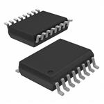
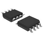
W25Q16BVSSIG NAND FLASH
IC FLASH 16MBIT SPI/QUAD 8SOIC
FLASH - NOR 存储器 IC 16Mb(2M x 8) SPI - 四 I/O 104 MHz 8-SOIC
16M-BIT SERIAL FLASH MEMORY WITH DUAL AND QUAD SPI
W25Q16BVSSIG NAND FLASH的技术参数:
|
制造商 |
Winbond Electronics |
|
包装 |
管件 |
|
存储器类型 |
非易失 |
|
存储器格式 |
闪存 |
|
技术 |
FLASH - NOR |
|
存储容量 |
16Mb(2M x 8) |
|
存储器接口 |
SPI - 四 I/O |
|
时钟频率 |
104 MHz |
|
写周期时间 - 字,页 |
50μs,3ms |
|
电压 - 供电 |
2.7V ~ 3.6V |
|
工作温度 |
-40°C ~ 85°C(TA) |
|
安装类型 |
表面贴装型 |
|
封装/外壳 |
8-SOIC(0.209",5.30mm 宽) |
|
供应商器件封装 |
8-SOIC |
W25Q16BVSSIG NAND FLASH的描述
The W25Q16BV (16M-bit) Serial Flash memory provides a storage solution for systems with limited space, pins and power. The 25Q series offers flexibility and performance well beyond ordinary Serial Flash devices. They are ideal for code shadowing to RAM, executing code dire
ctly from Dual/Quad SPI (XIP) and storing voice, text and data. The devices operate on a single 2.
7V to 3.6V power supply with current consumption as low as 4mA active and 1μA for power-down. All devices are offered in space-saving packages.
The W25Q16BV array is organized into 8,192 programmable pages of 256-bytes each. Up to 256 bytes can be programmed at a time. Pages can be erased ingroups of 16 (sector erase), groups of 128 (32KB block erase), groups of 256 (64KB block erase) or the entire chip (chip erase). The W25Q16BV has 512 erasable sectors and 32 erasable blocks respectively.
The small 4KB sectors allow for greater flexibility in applications that require data and parameter storage.The W25Q16BV supports the standard Serial Peripheral Interface (SPI), and a high performance Dual/Quad output as well as Dual/Quad I/O SPI: Serial Clock, Chip Select, Serial Data I/O0 (DI), I/O1 (DO), I/O2 (/WP), and I/O3 (/HOLD). SPI clock frequencies of up to 104MHz are supported allowing equivalent clock rates of 208MHz for Dual Outputand 416MHz for Quad Output when using the Fast Read Dual/Quad Output instructions.
These transfer rates can outperform standard Asynchronous 8 and 16-bit Parallel Flash memories. The Continuous Read Mode allows for efficient memory access with as few as 8-clocks of instruction-overhead to read a 24-bit address, allowing true XIP (execute in place) operation. A Hold pin, Write Protect pin and programmable write protection, with top or bottom array control, provide further control flexibility. Additionally, the device supports JEDEC standard manufacturer and device identification with a 64-bit Unique Serial Number.


 询价
询价