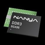
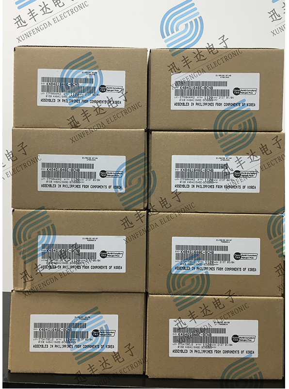
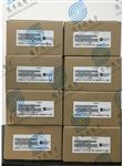
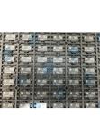
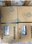
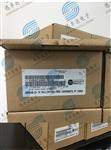
全新原装K4B4G1646E-BCNB DDR3 4Gb SAMSUNG/三星 1066 MHZ 256Mx16 存储器
全新原装K4B4G1646E-BCNB DDR3 存储器4Gb 的技术参数:
脚位/封装FBGA-96
无铅/环保无铅/环保
电压(伏)1.5 V
温度规格0°C~+85°C
速度1066 MHZ
标准包装数量1120
Number Of Words256M
Bit Organizationx16
Density4G
全新原装K4B4G1646E-BCNB DDR3 存储器4Gb 的 关键特性:
•JEDEC standard 1.5V(1.425V~1.575V)
•VDDQ = 1.5V(1.425V~1.575V)
•400 MHz fCK for 800Mb/sec/pin, 533MHz fCK for 1066Mb/sec/pin, 667MHz fCK for 1333Mb/sec/pin, 800MHz fCK for 1600Mb/sec/pin, 933MHz fCK for 1866Mb/sec/pin, 1066 MHz fCK for 2133Mb/sec/pin
•8 Banks
•Programmable CAS Latency(posted CAS): 5,6,7,8,9,10,11,13,14
•Programmable Additive Latency: 0, CL-2 or CL-1 clock
•Programmable CAS Write Latency (CWL) = 5 (DDR3-800), 6 (DDR3-1066), 7 (DDR3-1333) , 8 (DDR3-1600), 9 (DDR3-1866) and 10 (DDR3-2133)
•8-bit pre-fetch
•Burst Length: 8 , 4 with tCCD = 4 which does not allow seamless read or write [either On the fly using A12 or MRS]
•Bi-directional Differential Data-Strobe
•Internal(self) calibration : Internal self calibration through ZQ pin (RZQ : 240 ohm±1%)
•On Die Termination using ODT pin
•Average Refresh Period 7.8us at lower than TCASE 85°C, 3.9us at 85°C < TCASE < 95°C
•Asynchronous Reset
•Package : 96 balls FBGA - x16
•All of Lead-Free products are compliant for RoHS
•All of products are Halogen-free

The 4Gb DDR3 SDRAM E-die is organized as a 32Mbit x 16 I/Os x 8banks,device. This synchronous device achieves high speed double-data-rate transfer rates of up to 2133Mb/sec/pin (DDR3-2133) for general applications.
The chip is designed to comply with the following key DDR3 SDRAM features such as posted CAS, Programmable CWL, Internal (Self) Calibration,On Die Termination using ODT pin and Asynchronous Reset .
All of the control and address inputs are synchronized with a pair of externally supplied differential clocks. Inputs are latched at the crosspoint of differential clocks (CK rising and CK falling). All I/Os are synchronized with a pair of bidirectional strobes (DQS and DQS) in a source synchronous fashion. The address bus is used to convey row, column and bank address
information in a RAS/CAS multiplexing style. The DDR3 device operates with a single 1.5V(1.425V~1.575V)power supply and 1.5V(1.425V~1.575V) VDDQ.
The 4Gb DDR3 E-die device is available in 96ball FBGAs(x16).
全新原装K4B4G1646E-BCNB DDR3 存储器4Gb
K4B4G1646E-BCNB DDR3


 询价
询价